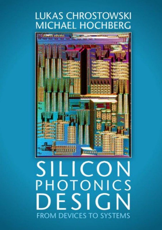
Silicon Photonics Design From Devices to Systems 1st Edition by Lukas Chrostowski, Michael Hochberg 1107085454 9781107085459
$50.00 Original price was: $50.00.$25.00Current price is: $25.00.
Authors:Lukas Chrostowski; Michael Hochberg , Series:Physics [3] , Tags:Science; Physics; Optics & Light; Technology & Engineering; Electronics; General; Optoelectronics; Optics , Author sort:Chrostowski, Lukas & Hochberg, Michael , Ids:9781107085459 , Languages:Languages:eng , Published:Published:Mar 2015 , Publisher:CAMBRIDGE UNIVERSITY PRESS , Comments:Comments:From design and simulation through to testing and fabrication, this hands-on introduction to silicon photonics engineering equips students with everything they need to begin creating foundry-ready designs. In-depth discussion of real-world issues and fabrication challenges ensures that students are fully equipped for careers in industry. Step-by-step tutorials, straightforward examples, and illustrative source code fragments guide students through every aspect of the design process, providing a practical framework for developing and refining key skills. Offering industry-ready expertise, the text supports existing PDKs for CMOS UV-lithography foundry services (OpSIS, ePIXfab, imec, LETI, IME and CMC) and the development of new kits for proprietary processes and clean-room based research. Accompanied by additional online resources to support students, this is the perfect learning package for senior undergraduate and graduate students studying silicon photonics design, and academic and industrial researchers involved in the development and manufacture of new silicon photonics systems.
Silicon Photonics Design From Devices to Systems 1st Edition by Lukas Chrostowski, Michael Hochberg – Ebook PDF Instant Download/Delivery. 1107085454, 9781107085459
Full download Silicon Photonics Design From Devices to Systems 1st Edition after payment
Product details:
ISBN 10: 1107085454
ISBN 13: 9781107085459
Author: Lukas Chrostowski; Michael Hochberg
From design and simulation through to testing and fabrication, this hands-on introduction to silicon photonics engineering equips students with everything they need to begin creating foundry-ready designs. In-depth discussion of real-world issues and fabrication challenges ensures that students are fully equipped for careers in industry. Step-by-step tutorials, straightforward examples, and illustrative source code fragments guide students through every aspect of the design process, providing a practical framework for developing and refining key skills. Offering industry-ready expertise, the text supports existing PDKs for CMOS UV-lithography foundry services (OpSIS, ePIXfab, imec, LETI, IME and CMC) and the development of new kits for proprietary processes and clean-room based research. Accompanied by additional online resources to support students, this is the perfect learning package for senior undergraduate and graduate students studying silicon photonics design, and academic and industrial researchers involved in the development and manufacture of new silicon photonics systems.
Silicon Photonics Design From Devices to Systems 1st Table of contents:
Part I Introduction
1 Fabless silicon photonics
1.1 Introduction
1.2 Silicon photonics: the next fabless semiconductor industry
1.2.1 Historical context – Photonics
1.3 Applications
1.3.1 Data communication
1.4 Technical challenges and the state of the art
1.4.1 Waveguides and passive components
1.4.2 Modulators
1.4.3 Photodetectors
1.4.4 Light sources
1.4.5 Approaches to photonic–electronic integration
Monolithic integration
Multi-chip integration
1.5 Opportunities
1.5.1 Device engineering
1.5.2 Photonic system engineering
A transition from devices to systems
1.5.3 Tools and support infrastructure
Electronic–photonic co-design
DFM and yield management
1.5.4 Basic science
1.5.5 Process standardization and a history of MPW services
ePIXfab and Europractice
IME
OpSIS
CMC Microsystems
Other organizations
References
2 Modelling and design approaches
2.1 Optical waveguide mode solver
2.2 Wave propagation
2.2.1 3D FDTD
FDTD modelling procedure
2.2.2 2D FDTD
2.2.3 Additional propagation methods
2D FDTD with Effective Index Method
Beam Propagation Method (BPM)
Eigenmode Expansion Method (EME)
Coupled Mode Theory (CMT)
Transfer Matrix Method (TMM)
2.2.4 Passive optical components
2.3 Optoelectronic models
2.4 Microwave modelling
2.5 Thermal modelling
2.6 Photonic circuit modelling
2.7 Physical layout
2.8 Software tools integration
References
Part II Passive components
3 Optical materials and waveguides
3.1 Silicon-on-insulator
3.1.1 Silicon
Silicon – wavelength dependence
Silicon – temperature dependence
3.1.2 Silicon dioxide
3.2 Waveguides
3.2.1 Waveguide design
3.2.2 1D slab waveguide – analytic method
3.2.3 Numerical modelling of waveguides
3.2.4 1D slab – numerical
Convergence tests
Parameter sweep – slab thickness
3.2.5 Effective Index Method
3.2.6 Effective Index Method – analytic
3.2.7 Waveguide mode profiles – 2D calculations
3.2.8 Waveguide width – effective index
3.2.9 Wavelength dependence
3.2.10 Compact models for waveguides
3.2.11 Waveguide loss
3.3 Bent waveguides
3.3.1 3D FDTD bend simulations
3.3.2 Eigenmode bend simulations
3.4 Problems
3.5 Code listings
References
4 Fundamental building blocks
4.1 Directional couplers
4.1.1 Waveguide mode solver approach
Coupler-gap dependence
Coupler-length dependence
Wavelength dependence
4.1.2 Phase
4.1.3 Experimental data
4.1.4 FDTD modelling
FDTD versus mode solver
4.1.5 Sensitivity to fabrication
4.1.6 Strip waveguide directional couplers
4.1.7 Parasitic coupling
Delta beta coupling
4.2 Y-branch
4.3 Mach–Zehnder interferometer
4.4 Ring resonators
4.4.1 Optical transfer function
4.4.2 Ring resonator experimental results
4.5 Waveguide Bragg grating filters
4.5.1 Theory
Grating coupling coefficient
4.5.2 Design
Transfer Matrix Method
Grating physical structure design
Modelling gratings using FDTD
4.5.3 Experimental Bragg gratings
Strip waveguide gratings
Rib waveguide gratings
Grating period
4.5.4 Empirical models for fabricated gratings
Computation lithography models
Additional fabrication considerations
4.5.5 Spiral Bragg gratings
Thermal sensitivity
4.5.6 Phase-shifted Bragg gratings
4.5.7 Multi-period Bragg gratings
4.5.8 Grating-assisted contra-directional couplers
4.6 Problems
4.7 Code listings
References
5 Optical I/O
5.1 The challenge of optical coupling to silicon photonic chips
5.2 Grating coupler
5.2.1 Performance
5.2.2 Theory
5.2.3 Design methodology
Analytic grating coupler design
Design using 2D FDTD simulations
Results
Design parameters
Cladding and buried oxide
Compact design – focusing
Mask layout
3D simulation
5.2.4 Experimental results
5.3 Edge coupler
5.3.1 Nano-taper edge coupler
Mode overlap calculation approach
FDTD approach
5.3.2 Edge coupler with overlay waveguide
Eigenmode expansion method
5.4 Polarization
5.5 Problems
5.6 Code listings
References
Part III Active components
6 Modulators
6.1 Plasma dispersion effect
6.1.1 Silicon, carrier density dependence
6.2 pn-Junction phase shifter
6.2.1 pn-Junction carrier distribution
6.2.2 Optical phase response
6.2.3 Small-signal response
6.2.4 Numerical TCAD modelling of pn-junctions
6.3 Micro-ring modulators
6.3.1 Ring tuneability
6.3.2 Small-signal modulation response
6.3.3 Ring modulator design
6.4 Forward-biased PIN junction
6.4.1 Variable optical attenuator
6.5 Active tuning
6.5.1 PIN phase shifter
6.5.2 Thermal phase shifter
6.6 Thermo-optic switch
6.7 Problems
6.8 Code listings
References
7 Detectors
7.1 Performance parameters
7.1.1 Responsivity
7.1.2 Bandwidth
Transit time
RC response
Dark current
7.2 Fabrication
7.3 Types of detectors
7.3.1 Photoconductive detector
7.3.2 PIN detector
7.3.3 Avalanche detector
Charge region design
7.4 Design considerations
7.4.1 PIN junction orientation
7.4.2 Detector geometry
Detector length
Detector width
Detector height
7.4.3 Contacts
Contact material
Contact geometry
7.4.4 External load on the detector
7.5 Detector modelling
7.5.1 3D FDTD optical simulations
7.5.2 Electronic simulations
7.6 Problems
7.7 Code listings
References
8 Lasers
8.1 External lasers
8.2 Laser modelling
8.3 Co-packaging
8.3.1 Pre-made laser
8.3.2 External cavity lasers
8.3.3 Etched-pit embedded epitaxy
8.4 Hybrid silicon lasers
8.5 Monolithic lasers
8.5.1 III–V Monolithic growth
8.5.2 Germanium lasers
8.6 Alternative light sources
8.7 Problem
References
Part IV System design
9 Photonic circuit modelling
9.1 Need for photonic circuit modelling
9.2 Components for system design
9.3 Compact models
9.3.1 Empirical or equivalent circuit models
9.3.2 S-parameters
9.4 Directional coupler – compact model
9.4.1 FDTD simulations
9.4.2 FDTD S-parameters
Directional coupler S-parameters
9.4.3 Empirical model – polynomial
9.4.4 S-parameter model passivity
Passivity assessment
Passivity enforcement
9.5 Ring modulator – circuit model
9.6 Grating coupler – S-parameters
9.6.1 Grating coupler circuits
9.7 Code listings
References
10 Tools and techniques
10.1 Process design kit (PDK)
10.1.1 Fabrication process parameters
Silicon thickness and etch
GDS layer map
Design rules
10.1.2 Library
10.1.3 Schematic capture
10.1.4 Circuit export
10.1.5 Schematic-driven layout
10.1.6 Design rule checking
10.1.7 Layout versus schematic
10.2 Mask layout
10.2.1 Components
10.2.2 Layout for electrical and optical testing
10.2.3 Approaches for fast GDS layout
10.2.4 Approaches for space-efficient GDS layout
References
11 Fabrication
11.1 Fabrication non-uniformity
11.1.1 Lithography process contours
11.1.2 Corner analysis
11.1.3 On-chip non-uniformity, experimental results
Ring resonators
Grating couplers
11.2 Problems
References
12 Testing and packaging
12.1 Electrical and optical interfacing
12.1.1 Optical interfaces
Grating couplers
Edge couplers
Individual fibres
Spot-size converter
Fibre array
Free-space coupling
Fibre taper coupling
12.1.2 Electrical interfaces
Bond pads
Probing
Wire bonding
Flip-chip bonding
12.2 Automated optical probe stations
12.2.1 Parts
Sample stage
Fibre array probe
Electrical probes
Microscopes
12.2.2 Software
12.2.3 Operation
Loading and aligning a chip/wafer
Aligning the fibre array
Chip registration
Automated device testing
12.2.4 Optical test equipment
12.3 Design for test
12.3.1 Optical power budgets
12.3.2 Layout considerations
12.3.3 Design review and checklist
References
13 Silicon photonic system example
13.1 Wavelength division multiplexed transmitter
13.1.1 Ring-based WDM transmitter architectures
13.1.2 Common-bus WDM transmitter
13.1.3 Mod-Mux WDM transmitter
13.1.4 Conclusion
People also search for Silicon Photonics Design From Devices to Systems 1st:
silicon photonics design from devices to systems free pdf
silicon photonics fundamentals and devices pdf
4h-silicon-carbide-on-insulator for integrated quantum and nonlinear photonics
silicon photonics design from devices to systems by lukas chrostowski
You may also like…
eBook EPUB
Introduction to Game Systems Design 1st Edition by Dax Gazaway ISBN 9780137440788 0137440782
eBook PDF
Functional Occlusion From TMJ to Smile Design 1st edition by Peter Dawson 9780323078986 0323078982


